
NPU IP
Compute meets memory.
A complementary architecture combining the low-power characteristics of PIM (Processing-in-Memory) with the high reconfigurability of an NPU. Rather than relying solely on automated EDA placement and routing, we use manual physical design to place compute units and memory close together. Minimizing data movement reduces energy consumption, computation time and chip area through PPA optimization.
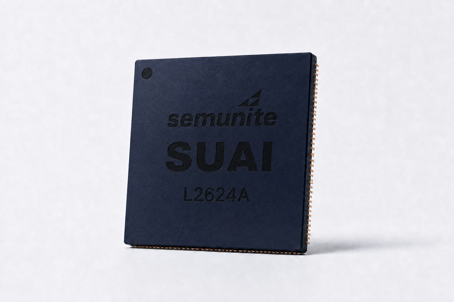
PIM-like NPU IP
- Manual physical design
- Place compute and memory close together to minimize data movement
- PPA optimization
- Reduce energy consumption, computation time and chip area together
- Post-simulation and measurement
- Simulation results obtained · Accredited-lab measurements in progress
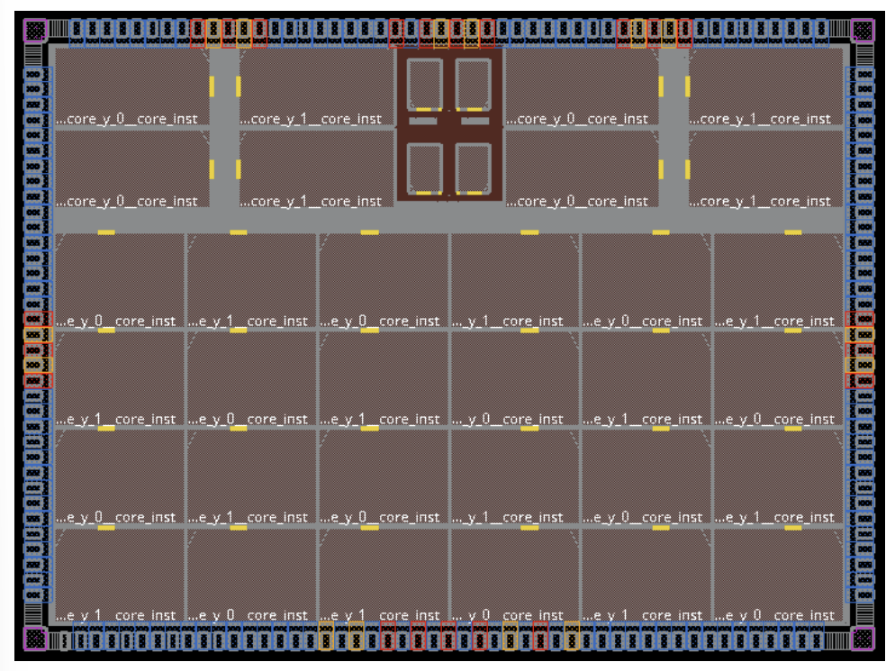
Validation status
SUAI test chips support validation of the NPU architecture in physical hardware.
6–8 TOPS/W · Post-simulation result
0.45 TOPS · 400 MHz · 8-bit × 8-bit integer operations (INT8 × INT8) · Accredited-lab measurement in progress
Semunite presents this post-simulation result as world-leading energy efficiency. Accredited-lab measurements are ongoing; these figures are not final specifications for individual AI SoC products.
Read the CEO interview on technology and validation(new tab)Discuss NPU IP for your product.
Tell us about your model and product requirements.